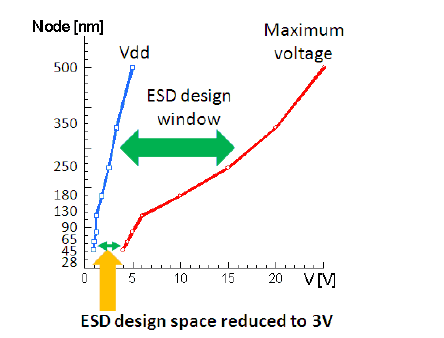
Esd Protection Device And Circuit Design For Advanced Cmos Technologies
 Esd Protection Device And Circuit Design For Advanced Cmos
esd protection device and circuit design for advanced cmos technologies is important information accompanied by photo and HD pictures sourced from all websites in the world. Download this image for free in High-Definition resolution the choice "download button" below. If you do not find the exact resolution you are looking for, then go for a native or higher resolution.
Don't forget to bookmark esd protection device and circuit design for advanced cmos technologies using Ctrl + D (PC) or Command + D (macos). If you are using mobile phone, you could also use menu drawer from browser. Whether it's Windows, Mac, iOs or Android, you will be able to download the images using download button.

 Esd Protection Device And Circuit Design For Advanced Cmos
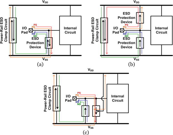
 Esd Design And Optimization In Advanced Cmos Soi Technology
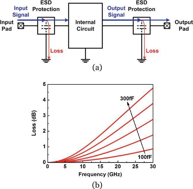
 Low C Esd Protection Design In Cmos Technology Intechopen

 Figure 7 From Esd Protection Circuit Design For Ultra
 Low C Esd Protection Design In Cmos Technology Intechopen
 Esd Protection Device And Circuit Design For Advanced Cmos
 Figure 3 From Esd Protection Circuit Design For Ultra

 Esd Protection Device And Circuit Design For Advanced Cmos